Main features:
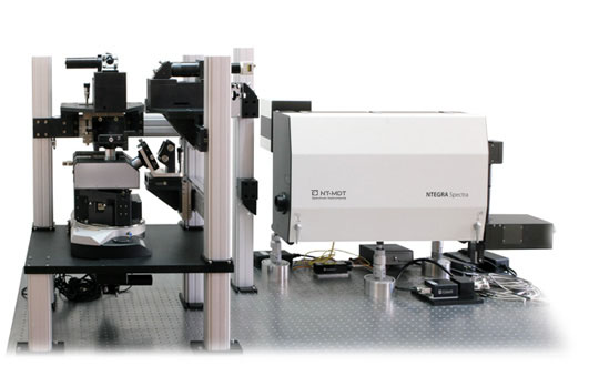
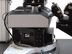
Since 1998 NT-MDT has been successfully integrating AFM with optical microscopy and spectroscopy techniques. More than 30 basic and advanced AFM modes including HybriD ModeTM are supported providing extensive information about the sample surface physical properties. Integration of AFM with confocal Raman/fluorescence microscopy provide the widest range of additional information about the sample.
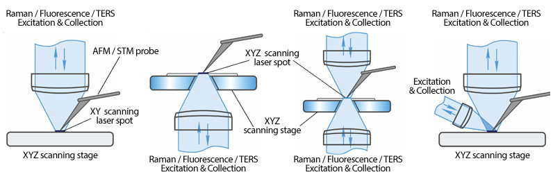
Simultaneously measured AFM and Raman maps of exactly the same sample area provide complementary information about sample physical properties (AFM) and chemical composition (Raman).
NTEGRA Spectra II with the help of Tip Enhanced Raman Scattering (TERS) allows carrying out spectroscopy/microscopy with nanometer scale resolution. Specially prepared AFM probes (nanoantennas) can be used for TERS to enhance and localize light at the nanometer scale area near the tip apex.
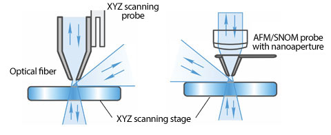
Such nanoantennas act as a “nano-source” of light giving possibility of optical imaging with resolution less than a diffraction limit (up to ~ 10 nm). Scanning near-field optical microscopy (SNOM) is another approach to obtain optical and spectroscopy images of optically active samples with resolution limited by probe aperture size (~ 100 nm).
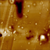
Graphene flakes
30x30 um
Ni foil
20x20 um
PC-PVAC film
30x30 um
MoO3
30x30 um
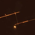
CdS nanowire was connected with metal electrode by conductive polymer nanowires. AFM probe is positioned on the structure with the help of viewing microscope. Thanks to the shape of the AFM probe laser can be positioned directly onto the tip apex.
High resolution AFM images provide information about sample topography. Raman and luminescence maps taken from the same area show difference in nanowires chemical composition.
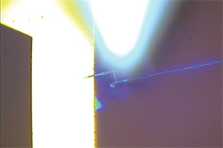
Optical viewing system image with approached AFM probe
Topography
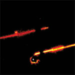
Raman map (conductive polymer nanowires)
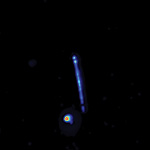
Photoluminescence (CdS)
Raman and PL spectrum of CdS nanowire
Topography
G band intensity

2D band intensity
Raman spectra
NT-MDT Spectrum Instruments has demonstrated enhancement of the Raman scattering (TERS) in application to an opaque sample - layer of organic dye deposed on a golden substrate - in liquid with the upright optical configuration NTEGRA Spectra II.
Implementation of TERS in liquid brings out some difficulties. The main one is the delicate optical alignment to achieve accurate focusing of the laser beam on the tip apex and also to ensure an efficient collection of the scattered signal especially through a layer of liquid. In case of transparent samples set on an inverted optical microscope focusing of the laser beam on the TERS probe is therefore easily achieved directly through the sample.
With opaque samples that require top or side illumination/collection, the optical signal is deviated and considerably attenuated by refraction at each interface.
One of the possible ways to avoid refraction on air-liquid surface and to achieve stable light path is to use immersion objective. NTEGRA Spectra II is the only instrument which provides such possibility as AFM beam deflection system works through the same objective as Raman laser.

During the experiment in AFM optical head a polarized excitation laser (λexc = 632.8 nm) was focused on the AFM TERS probe apex through a long distance 60× water immersion objective (working distance: 2 mm) with high numerical aperture (N.A. = 1). Therefore, the AFM tip holder can fit between the objective and the sample. Laser spot scanning was performed by scanning mirror.
The enhanced spectrum and the one obtained from tip apex are presented in the figure and confirm the strong enhancement of the signal from around the “hot-spot” location.
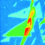
Ntegra Spectra II equipped with new electronics and software allows to combine a recently developed innovative HybriD Mode™ (HD-AFM™ Mode) for nanomechanical proprieties and Raman for chemical imaging of exactly the same area within single measurement session.
Stiffness of HDPE/LDPE polymer sandwich cut by microtome
Overlap of Raman maps: HDPE (red), LDPE (blue)
AFM topography

* Compatibility with other wavelength upon request
Tip Enhanced Raman Scattering (TERS, nano-Raman) is the technique for enhancement of weak Raman signals and for super-resolution Raman imaging with spatial resolution ~10 nm. Nano-Raman imaging provides unique insights into sample structure and chemical composition on the nanometer scale.
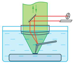
In TERS, a sharp metal probe (nano-antenna) is used to localize and enhance optical field at the tip apex (fig. 1a). The light enhancement is typically reached when excitation laser light is in resonance with localized surface plasmon at the end of the TERS probe (fig. 1b). Enhancement of electromagnetic field (light) intensity on the TERS probe apex can reach many orders of magnitudes. In TERS mapping the sample is scanned with respect to the nano-antenna; the enhanced Raman signal localized near the probe apex is measured resulting in Raman maps of the sample surface with nanometer scale resolution.
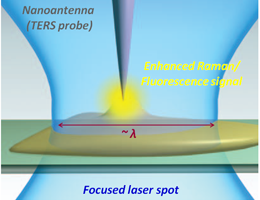
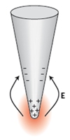
Fig.1. Principle of Tip Enhanced Raman Scattering and other tip- assisted optical techniques (left). Localized surface plasmon (electron density oscillations) at the end of a metal TERS probe (nano-antenna), resulting in light localization and enhancement at the probe apex (right).
NT-MDT develops and supplies unique instrumentation for AFM integration with various optical microscopy and spectroscopy techniques. NT-MDT was the first to introduce integrated AFM-Raman instrument in 1998 and is now the leading developer and supplier of such instruments worldwide.
NT-MDT AFM-Raman instrument has been successfully used for TERS (nano-Raman) mapping of various objects with spatial resolution reaching 10 nm: graphene and other carbon nanomaterials, polymers, thin molecular layers (including monolayers), semiconductor nanostructures, lipid membranes, various protein structures, DNA molecules etc. References to corresponding publications can be found at download page.
While the AFM-Raman instrumentation has been developing relatively fast, TERS probes have always remained main limiting factor for nano-Raman to become routine characterization technique. The main challenges are: (i) manufacturing reproducible probes with high enhancement factors and high resolution imaging capabilities; (ii) probe lifetime; (iii) probe ease of use; (iv) probe mass production not involving complicated and poorly reproducible manual procedures.
TERS probes originally used in scientific publications were usually etched metal wires - attached to tuning fork or working in STM (tunneling) regime. Preparation of such probes requires elaborated manual operations; probes are typically not very reproducible. Another approach to TERS probe preparation utilizes focused ion beam to manufacture special structure on the tip end. This approach is very resource consuming and also lacks reproducibility. Different metal coatings of AFM cantilevers have been reported recently – with different degrees of enhancements and reproducibility.
As a result of comprehensive research performed together with NT-MDT customers and partners, NT-MDT is now able to offer to its AFM-Raman customers mass produced reproducible cantilever-type TERS probes. The probes are prepared based on so-called “Top Visual” AFM Si cantilevers (Fig. 2). Special proprietary probe preparation and TERS metal coating are applied.
AFM probes can have different stiffness and can be optimized for contact and non-contact regimes.
Protruding “nose-type” shape of the probes allows Raman laser light to be focused on the probe apex from the top: for use with non-transparent samples.
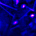
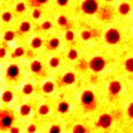
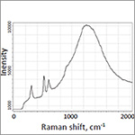
The probes provide guarantied TERS performance on a test sample (organic molecules on Au substrate):
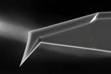
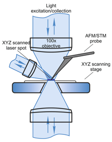
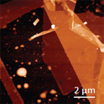
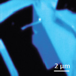
Fig. 2. SEM image of “Top Visual” AFM probe. Protruding probe geometry allows optical access to the apex from the top (left). Experimental TERS configuration (right).
The AFM TERS probes also feature excellent AFM performance in contact and non-contact regimes since they are prepared based on standard Si AFM cantilevers produced by mass technology. All advanced AFM modes (electrical, magnetic, nanomechanical etc.) are available with NT-MDT TERS probes. High resonance quality factors (for non-contact probes) allow excellent force sensitivity and guarantee long tip lifetime during measurements.
STM TERS probes (electrochemically etched metal wires) and TERS probes attached to tuning fork are also available.
The NT-MDT TERS probes reach their highest characteristics with the unique AFM-Raman instrument from NT-MDT: specifically designed for TERS research.
Probes are only supplied to be used with NT-MDT instrumentation. Contact us for more information.
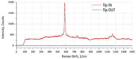
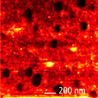
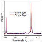
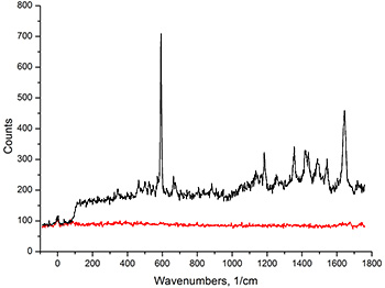
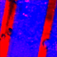
Fig. 3. Typical Raman signal enhancement (>100x) of NT-MDT TERS AFM probe (left). High resolution TERS map.
Resolution: ~20 nm. Sample: BCB thin molecular layer on Au substrate (right).
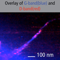
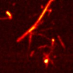
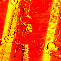
Fig. 4. High resolution TERS map of carbon nanotubes on Au substrate. Resolution: ~10 nm.
More technical information about TERS cantilevers: http://www.ntmdt-tips.com/products/group/ters-afm-probes-new