Interplay between Raman Scattering and Atomic Force Microscopy in Characterization of Polymer Blends
Application Note 094 (pdf 2 Mb, EN)
P. Dorozhkin, A.Shelaev and S.MagonovNT-MDT Co, Zelenograd, Moscow,
NT-MDT Development Inc.
INTRODUCTION
Atomic force microscopy (AFM) is routinely applied for compositional mapping of heterogeneous polymer materials. Recognition of the individual components in these materials is usually based on their specific morphology and differences of local mechanical and electric properties. Nowadays a deficit of local chemical or spectral information in AFM can be overcome by combining it with confocal Raman scattering microscopy [1, 2].
Such applications to polymer blends are fast developing and can be substantially enhanced with the use of multifrequency AFM techniques, which allow the simultaneous recording of surface morphology, local mechanical, dielectric and chemical (Raman spectra) responses from the same sample area. Initial efforts in this direction are presented in our work, which was focused on studies of films of immiscible blend of polystyrene (PS) and polyvinyl acetate (PVAC).
SAMPLE PREPARATION AND INSTRUMENTATION
Thin films of polymer blend of PS with PVAC (1:1, both with molecular weight of 100 K) were made by spin casting of their 1mg/ml solution in toluene. The film thickness varies in the 100‑140 nm range. Thick film of the same blend was prepared by slow air-drying of a droplet of the same solution. This film was thickness around 1 µm.
In both cases a conducting ITO glass was used as a substrate. The film thickness was determined by AFM measurements of the steps of the scratch made with in the films with a sharpened wooden stick. All materials were purchased from Sigma-Aldrich.

AFM, Kelvin probe force microscopy (KPFM, single-pass and double pass methods) and AFM-Raman studies were performed with NT-MDT microscope NTEGRA Spectra.
The AFM-Raman measurements were done in the upright geometry using 473 nm laser with a power of 3-9 mW and exposure from 0.4 to 20 sec and the objective 100x with NA 0.95.
RESULT
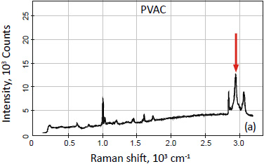
Our interest in PS-PVAC blends was brought about by recent efforts to measure its local dielectric properties by different AFM approaches [3‑5] and the fact that the Raman spectra of PS and PVAC are characterized by specific individual bands of these components (Fig. 1) that provide their direct recognition in confocal Raman maps obtained on the surface of the blend films. The static dielectric permittivity of the blend components are quite different (2-3 for PS and ca. 7 for PVAC) as well
as their dipole
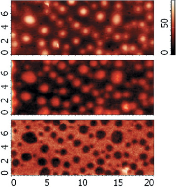
moments (ca. 0.30 for PS and 2.1D for PVAC). The constituents of this blend have different local electric properties (surface potential, dielectric permittivity) that is well documented in single-pass Kelvin probe force microscopy and dC/dZ studies. A comparison of the KPFM and dC/dZ images with Raman maps recorded at the same locations offers useful information about sensitivity as well as spatial and In-depth resolution of such characterization. The typical KPFM images of thin film of PS-PVAC blend are shown
in Fig. 2.
The height images reveal a phase-separated morphology with circular and elevated domains of the polar component immersed bright patches of these regions in surface potential, the strong dC/dZ contrast on these domains and their selective swelling in humid and methanol atmosphere [5].
The surface potential of the single PVAC domain shows that heterogeneity of this region. The latter can be related either to a presence of the nano-scale polymer assemblies differing in the orientation of their overalldipole moment or to some mixing of the components of this blend.
The analysis of the AFM and KPFM of the PS-PVAC films can get strong support from local spectroscopic studies. Remarkably, the Raman spectroscopy signalfrom thin film (around 140 nm in thickness) was good enough to generally prove the indirect assignment of surface domains to the individual blend components. This is seen in Fig. 3 where one sees topography and Raman maps for PS and PVAC components, which were obtained on a location similar to one shown in Fig. 2.
The compositional mapping of the morphology of thick PS-PVAC film has a particular benefit from the combined KPFM and Raman spectroscopy imaging as seen from Fig. 4. The surface depressions, which exhibit higher surface potential and brighter contrast in the Raman (PVAC) map, can be assigned to the polar constituent. Respectively, the elevated matrix is enriched in PS.
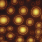
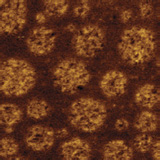
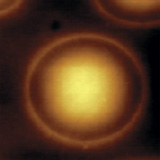
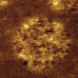
Fig. 2. Height and surface potential images of PS-PVAC thin film obtained in the single-pass KPFM studies.
This means that Raman spectroscopy reveals the under-surface material that is PVAC. This is not surprising because surface potential senses the top layer whereas the Raman spectroscopy detect the signalfrom sample with the focal depth is ~ 0.5 micron that is around half of the thickness of this film.
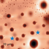
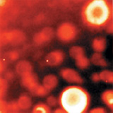
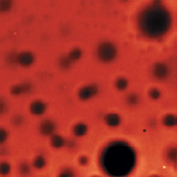
The Raman spectroscopy capability in detection of sub-surface composition has been also demonstrated at the other two locations of the thick PS-PVAC film, Figures 5-6. The high surface potentialis detected at the depressions of different size. In Fig. 5. Similar surface morphology has been observed in the another regions, Fig. 6.
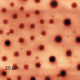
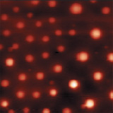
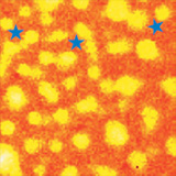
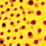
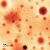
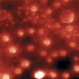
Fig. 5. Height and surface potential images of the thick film of PS-PVAC blend.
CONCLUSIONS
The combined use of Raman maps with AFM and KPFM data has provided the comprehensive analysis of PSPVAC blend in thin and thick films. The surface domains of the individual constituents were undoubtedly assigned, and the partial information regarding the sub-surface morphology has been also obtained.
The example demonstrates the strong potential of this approach for compositional mapping of heterogeneous polymer systems.
REFERENCES
[1]. 8.-S. Yeo eta Small 2009, 5, 952.
[2]. P. Dorozhkin et al, Microscopy Today 2010, 18, 28.
[3]. P .S. Crider et al, Appl. Phys. Lett. 2007, 91, 073102.
[4]. C. Riedel et al Appf. Phys. Lett. 2010, 96, 213110.
[5]. S. Magonov and J. Alexander, Beilstein Joum. Nanotechn. 2011, 2, 75.
