Non-destructive HybriD PFM study of diphenylalanine peptide nanotubes. From left to right: topography, adhesion,
Young’s modulus and in-plane piezoresponse phase. Scan size: 7×7 μm
Rebirth of Force Spectroscopy: HybriD AFM Mode. Webinar record
Application Note 095
"Exploring Imaging in Oscillatory Resonance AFM Modes: Backgrounds and Applications" (2,4 Mb).
Size: A4 or Letter
Application Note 087
"Expanding Atomic Force Microscopy with HybriD Mode Imaging" (8,8 Mb).
Size: A4 or Letter
HybriD mode (HD mode) – scanning technique based on fast force-distance curves measurements with real-time processing of tip response.
Measured properties:
In HybriD mode the tip-sample distance is modulated according to the quasi-harmonic law. Thus tip enters a force interaction with the sample thousands times per second. Force-distance curve analysis enables maps of topographical, nanomechanical, electrical, thermal and piezoelectric properties of the sample to be extracted with high spatial resolution and minimized lateral forces.
High-performance electronic components and unique algorithms implemented in the state-of-the-art HybriD 2.0 Control Electronics provide superb level of real-time signal processing and analysis. Combining mode with cutting-edge optical microscopy and spectroscopy techniques opens-up novel opportunities of cantilever-based tip-enhanced Raman scattering (TERS) and scattering scanning near-field optical microscopy (s-SNOM).
Force spectroscopy is a well-known AFM technique for quantification of local nanomechanical properties. HD mode allows fast, more than 1000 force curves per second measurements, real-time calculation of Young’s modulus according to Hertz, DMT, JKR and other mathematical models and automated cantilever force constant calibration.
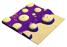
Polystyrene-polybutadiene blend on silicon substrate. Topography is overlaid by Young’s modulus maps. Scan size: 4×4 µm
HD mode ensures less than 10 nm spatial resolution of QNM maps.
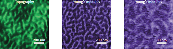
HD QNM study of PS-b-PMMA. Right image demonstrates around 10 nm spatial resolution
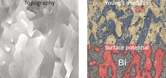
HD QNM study of Tin-Bismuth alloy. Scan size: 10×10 µm
HybriD Mode uniquely enables stiff materials to be distinguished from each other by means of an AFM probe. Areas corresponding to Bismuth (32 GPa, blue color) and Tin (50 GPa, yellow color) are clearly identified. The mechanical properties map corresponds well with the surface potential image.
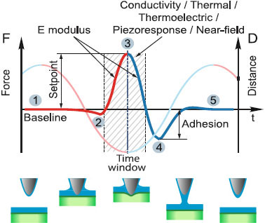
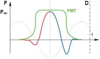
In HD Piezoresponse Force Microscopy mode (HD PFM) an AC voltage is applied to the conductive AFM cantilever when the tip comes in contact with the sample during each fast force spectroscopy cycle. Applied AC voltage causes mechanical oscillations of the piezoelectric (ferroelectric) sample.Corresponding vertical and lateral motions of the AFM tip are recorded and processed to get the amplitude and phase characterizing the local piezoelectric coefficient and local polarization direction respectively. Since the AFM tip retracts from the surface in each scanning point, the lateral tip-sample interaction force is significantly reduced in comparison to the conventional contact PFM technique.
This provides new capabilities for piezoresponse studies of soft, loose and fragile objects like biological samples, nanoparticles etc.
Furthermore an AFM cantilever of higher stiffness and resonance frequency can be used. Therefore the ability of two-pass resonant electrostatic measurements was implemented: Kelvin probe microscopy or Electrostatic force microscopy can be used simultaneously with topography, adhesion, E modulus and piezoresponse studies.
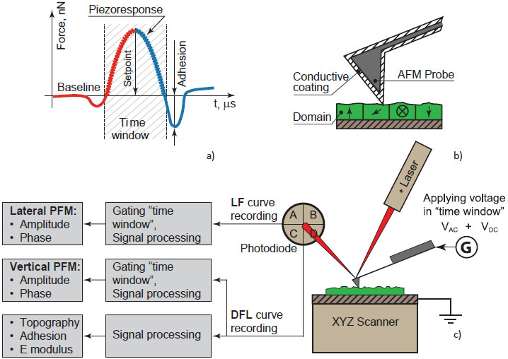
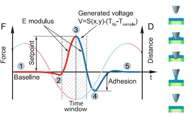
HD PFM working principle: a) an idealized temporal deflection curve during an oscillatory cycle, b) tip-sample interaction in “time window”, c) measurement scheme
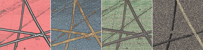
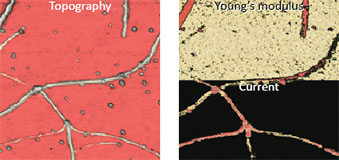
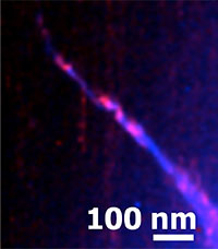
Non-destructive electromechanical study of diphenylalanine peptide nanotubes. Sample courtesy: Dr. A. Kholkin, University of Aveiro. Scan size: 7×7 µm, nanotubes diameter: 70÷100 nm
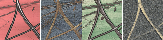
Non-destructive electromechanical study of diphenylalanine peptide nanotubes. Sample courtesy: Dr. A. Kholkin, University of Aveiro. Scan size: 8×8 µm, nanotubes diameter: 30÷150 nm
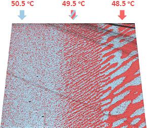
Topography of triglycine sulfate crystal overlaid with vertical piezoresponse phase. Image illustrates real-time observation of the second-order phase transition. The sample temperature was changed during scanning. Sample courtesy: Dr. R. Gainutdinov, IC RAS. Scan size: 15×15 µm
Another important characteristic of HybriD Piezoresponse Force Microscopy is its ability to perform electromechanical studies under varying temperature of the sample. A unique feature implemented in this mode is an automatic compensation of the thermal drift of the AFM probe at each point.
Electrical characterization of objects, that are weakly attached to the surface, has always been a challenge when using standard AFM modes like Conductive AFM. This was because often the tip moved or abraded the objects of interest. HybriD Mode drastically decreased the impact of lateral forces and simplified these experiments.
Comparison of conductive and mechanical maps shown in this example allows the clear identification of single nanotubes and bundles.
HD C-AFM study of carbon Nanotubes on Silicon. Sample courtesy: Dr. Kuljanishvili, Saint Louis University, Department of Physics. Scan size: 1×1 µm
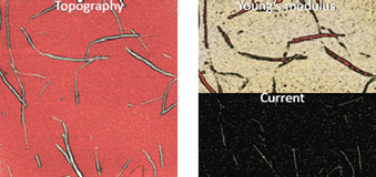
HD C-AFM study of coupled carbon and peptide nanotubes. Sample courtesy: Dr. J. Montenegro, University Santiago de Compostela. Scan size: 3×3 μm
New state-of-the-art HybriD 2.0 control electronics allows simultaneous resonant electrostatic studies using two-pass technique:
HD KPFM study of WS2 monolayers grown on epitaxial graphene measured in vacuum. Topography is overlaid with surface potential. Sample Courtesy: Dr. Cristina Giusca, NPL, Prof. Mauricio Terrones, PSU. Scan size: 14×14 µm
Thermoelectric studies of nanoscale structures like n-p junctions, conductive nanowires, graphene oxide etc. are currently of a great interest. HD Scanning Thermoelectric Microscopy (HD SThEM) allows non-destructive mapping of Seebeck coefficient with tip radius-limited spatial resolution. HD SThEM working principle is based on direct measurement of generated voltage when conductive tip and sample under different temperatures contact each other during fast force spectroscopy measurements.
HD Scanning Thermoelectric Microscopy working principle,V – generated voltage, S(x,y) – Seebeck coefficient
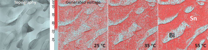
HD SThEM study of Tin-Bismuth alloy. Seebeck coefficient, S: Bi -72 mV/C, Sn -1.5 mV/C. Scan size: 7×7 µm
High resolution TERS map of carbon nanotubes on Au substrate. Resolution: ~10 nm. Overlay of G-band (blue) and D-band (red)
Tip Enhanced Raman Scattering (TERS, nano-Raman) is the technique for enhancement of weak Raman signals and for super-resolution Raman imaging with spatial resolution less than 10 nm.
As a result of comprehensive research performed together with NT-MDT China customers and partners, we are now able to offer to AFM-Raman customers mass produced reproducible TERS probes.
TERS imaging requires prolonged tip-sample contact at each scanning point but Contact AFM is destructive for both the tip and the sample. Thereby, HD mode is a superior technique for cantilever-type TERS since it noticably increases the tip lifetime and makes possible TERS imaging of soft, loose and fragile samples.
Thanks to high-speed HybriD 2.0 Control Electronics the approach and withdrawal optical response signal curve (PMT) can be recorded and processed in real-time. This allows to separate a near-field from far-field component of optical response and to map it spatial resolution limited by the tip radius.
Here we demonstrate its application to PS/PBD polymer blend study with less than 100 nm optical resolution.
HD s-SNOM working principle
HD s-SNOM study of PS/PBD film

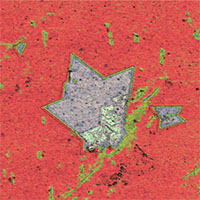
Bio HD study of Stem Cell fragment in Liquid. Elastic Modulus range: 0.2-1.5 kPa. Scan size: 18×30 µm
Tip Enhanced Raman Scattering (TERS, nano-Raman) is the technique for enhancement of weak Raman signals and for super-resolution Raman imaging with spatial resolution less than 10 nm.
As a result of comprehensive research performed together with NT-MDT China customers and partners, we are now able to offer to AFM-Raman customers mass produced reproducible TERS probes.
TERS imaging requires prolonged tip-sample contact at each scanning point but Contact AFM is destructive for both the tip and the sample. Thereby, HD mode is a superior technique for cantilever-type TERS since it noticably increases the tip lifetime and makes possible TERS imaging of soft, loose and fragile samples.
Vacuum measurements in amplitude modulation (AM) mode requires unacceptably low scanning speeds because of extremely high Q-factor of AFM probes. Being a non-resonant mode, HD mode allows at least 10 times faster imaging speed.
Another issue of AM mode in vacuum is that it is influenced by the electrostatic forces while the HD mode working principle allows automatic compensation of long-distance forces at each scanning point.
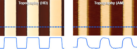
Topography of TGZ2 calibration grating measured in vacuum with use of HD and AM modes. Scanning speed is 1 Hz. Grating period is 3 µm, height is 100 nm
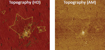
WS2 monolayers grown on epitaxial graphene measured in vacuum with use of HD and AM modes. The influence of electrostatic forces is demonstrated.
Sample Courtesy: Dr. Cristina Giusca, NPL, Prof. Mauricio Terrones, PSU.
Scan size: 14×14 µm
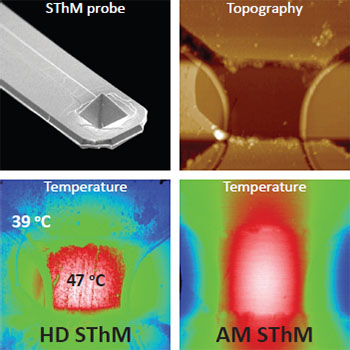
SEM image of AppNano VertiSense™ thermocouple probe and comparison of HD SThM and AM SThM techniques. Scan size: 17×17 µm.
HD Scanning Thermal Microscopy (HD SThM) allows studying local thermal properties simultaneously with QNM measurements. From the hardware point of view it was implemented using AppNano VertiSense™ thermocouple probes. The thermal conductivity and temperature mapping modes (CMM, TMM) can be realized by positioning the AFM laser at the end or the central part of the probe, respectively. HD mode working principle allows exceptional spatial resolution of SThM measurements in comparison to conventional Amplitude Modulation (AM) mode. That was demonstrated in TMM of a micro-heater sample.
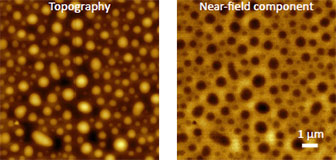
SThM and HybriD mode is the winning combination for distinguishing between the constituents of polymer blends as demonstrated in the example of a blend of polystyrene (PS) with low density polyethylene (LDPE) (see below). The difference in thermal conductivity of the polymers (PS – 0.12 W/mK; LDPE – 0.33 W/mK) allows the assignment of the colder matrix to LDPE and the hotter islands to PS.
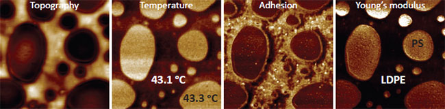
HD SThM study of PS-LDPE. Scan size: 10×10 μm
State-of-the-art HybriD 2.0 Control Electronics incorporates high-speed digital lock-in amplifiers (LIA) and phase locked loop detector (PLL) for advanced oscillatory resonance modes: Amplitude Modulation with Frequency Imaging (AM-FI) and Frequency Modulation (FM) modes. They provide exceptional level of spatial resolution of challenging flat and soft samples (self-assembled molecular structures etc.) thanks to ultra-precise control of the tip-sample interaction force. Additionally they allow mapping of its mechanical properties.
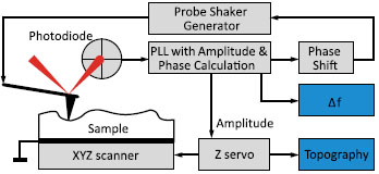
Schematics of AM-FI mode
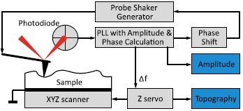
Schematics of FM mode
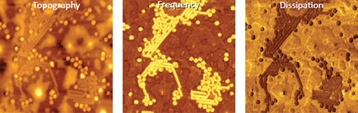
The two images below show topography and probe resonant frequency distribution over lamellar arrangement of short alkane C36H74 on graphite with a spacing of 4.5 nm. One can also see a couple of adsorbates formed on the lamellar surface by disordered alkane chains which are rarely observed by the traditional AM mode.
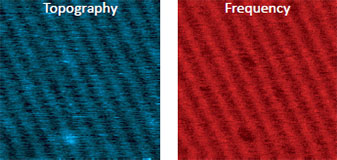
AM- FI mode images of C36H74 lamellae on graphite. Scan size 40×40 nm
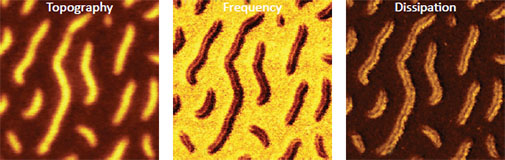
FM mode images of brush-like macromolecules on mica. Scan size 500×500 nm
AM-FI mode images of F14H20 adsorbate on graphite. Scan size 1.5×1.5 µm
| Parameter | Value |
| High Speed ADC-s | 2 × 20 MHz, 16 bit |
| High Precision ADC-s | 4 × 1 MHz, 18 bit |
| DAC-s | 20 × 16 bit 1 MHz 2 × 12 bit 20 MHz |
| FPGA | 120 MHz, Floating Point |
| DDS (Direct digital synthesizer) | 2 × 20 MHz |
| Lock-in Amplifier Band | 4 MHz |
| High Voltage Amplifier | ±150 V, slew rate 32 V/uSec.(limited to 33 kHz at 150 V) small signal bandwidth 500 kHz at < 10 V Amplitude |
| Number of curves per second | Limited only by Z scanner resonance frequency |
| PLL | |
| Operational Modes | Self-exciting oscillation, constant amplitude, constant excitation |
| Measurement Resolution | 0,3 Hz at 10 kHz BW; 0,02 Hz at 600 Hz BW |
| Demodulation Bandwidth | 500 kHz |
| Digital Phase Shifter | 0 – 360˚ (20 bit); 0,34 millidegree step |
| Spectrum Analysis | Amplitude, Phase |
| Probe Safety | Yes |
| Output Modulation | p-p 10V with 0,15 mV resolution |
| Input Signal | 10 kHz - 1 MHz; 70 mV - 10 V |
| Common | |
| PC Interface | USB 2.0, Ethernet |
| Program SDK | LabView |
| Power Supply | 100-240 V (50/60 Hz) |
| Set of modes | |
| Topography, Elastic modulus, Lift and Land Adhesion, Work of Adhesion, Current, Force Volume, PFM, KPFM, MFM, EFM | |